
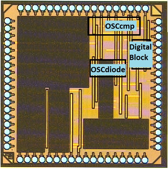
This test chip demonstrates a high-stability ultra-low-power on-chip clock source platform. It consists of an ultra-low-power diode-based temperature-uncompensated oscillator (OSCdiode) that frequency locks to a higher-power temperature-compensated oscillator (OSCcmp), which is disabled after each locking event to save power. The locking allows the stability of the uncompensated oscillator to stay within the stability bound of the compensated design. A digital block is able to control the locking interval using a periodic (counter-based) scheme that was implemented on-chip and a prediction (temperature drift-based) scheme that was verified off-chip. The clock source system was implemented in a 130 nm CMOS technology. It achieves a high effective long-term temperature stability of 7 ppm/°C from 20°C to 40°C (20 ppm/°C from 20°C to 70°C), with a power consumption of 36 nW at 0.7 V.