
Projects
Categories of projects in the RLPVLSI Group

A 1 trillion node internet of things (IoT) will require sensing platforms that support numerous applications using power harvesting to avoid the cost and scalability challenge of battery replacement in such large numbers. Our previous SoCs achieve good integration and energy harvesting, but they limit supported applications, need higher end-to-end harvesting efficiency, and require duty-cycling for RF communication. In this project, we demonstrates a highly integrated, flexible SoC platform that supports multiple sensing modalities, extracts information from data flexibly across applications, harvests and delivers power efficiently, and communicates wirelessly.
 |
Enabling self-powered in-fiber or in-textile sensing systems necessitates the development of a compact, highly expandable, and ultra-low-power (ULP) communication protocol. This work presents an ULP “bypass-SPI” chip-to-chip interconnect bus designed specifically for fabric-based network communication, requiring only a fixed set of four wires. This interconnect bus allows the chips to bypass the interconnect signals to the downstream chips using a dedicated bypass procedure, facilitating small form factors. A voltage and direction controller is integrated on-chip, which allows the expansion of interconnect signals in multiple directions, supporting mesh-style distributed fiber networks and enabling voltage shifting. Moreover, this interconnect bus is synthesizable, compatible with the standard SPI interfaces, and can be converted into an I2C protocol, significantly improving its flexibility. Fabricated in 65nm CMOS technology, measurements of the chip show that the chip achieves a minimum standby power of 2.3 nW and reduces the energy per cycle by over 17× down to 1 pJ/bit, compared to prior art. The communication between bypass-SPI chips and a RISC-V SoC is also measured, confirming the suitability of this interconnect bus for energy-and-space-constrained fabric-based sensing applications. |
 |
Advancements in power and size reduction for integrated circuits (IC) enable integration of self-powered systems into mm-scale fiber strand. Moving towards intricate fiber networks where multiple subsystems interact within textiles or garments, energy harvesting and power management units (EHPMU) require full autonomy, ultra-low quiescent power, high efficiency, and a mm-scale footprint. Additionally, they must coordinate energy across distributed subsystems for enhanced system viability and scalability. A switched-capacitor (SC) based ultra-low-power (ULP) EHPMU [1] realizes distributed energy sharing but its cascade structure restricts the efficiency and dynamic range (<5µW). Also, its single-rail-sharing architecture for distributed systems forces all subsystems to interact with a shared rail, necessitating extra dedicated converters, thereby increasing cost. Existing multi-input single-inductor multi-output (MISIMO) EHPMUs [2-7] achieve high efficiency with a single power-delivery stage, but they either consume >100nW quiescent power [3-7], have <1000× dynamic range [3][5], lack full autonomy [3][4][6][7], or require large inductor (22µH) with low efficiency due to conventional buck-boost (CBB) conversion [2]. Furthermore, none of them support distributed systems. As shown in the top of Fig. 1, we address these limitations with a fully autonomous triple-input hybrid-inductor-capacitor multi-output (TIHICMO) EHPMU that can harvest energy from dual input sources, regulate three custom output rails, adaptively switch among multi-conversion methods, cold startup (CS) from all the inputs/outputs, and enable energy recycling and sharing among multiple rails. This EHPMU achieves a 5.8nA quiescent current, a wide dynamic range of 8.8x10⁴, a peak efficiency of 90.1%, and a >90% reduction in inductor size compared to [2][7] using a 3×3×1.3mm 200mΩ DCR inductor. |
 |
This work presents a fully autonomous system-on-chip (SoC) that can be distributed along a fiber strand, capable of simultaneously harvesting energy, cooperatively scaling performance, sharing power, and booting-up with other in-fiber SoCs for ultra-low-power (ULP) sensing applications. Utilizing a custom switched capacitor energy harvesting and power management unit (EHPMU), the SoC can efficiently redistribute and reuse harvested energy along the fiber. Integrated on-chip, the ULP RISC-V digital core and temperature sensor enable energy-efficient sensing and computation at nanowatt power levels. A dedicated ripple boot-up and cooperative dynamic voltage and frequency scaling (DVFS) further optimize the operation and physical size of the system. Fabricated in 65 nm, measurement results show that the proposed SoC achieves 33 nW power consumption for the whole chip under 92 Lux lighting condition and can reduce control power down to 2.7 nW for the EHPMU. With the proposed power sharing and cooperative DVFS techniques, the SoC reduces the illuminance needed to stay alive by >7× down to 12 Lux. Integrated into a mm-scale polymer fiber, our SoC demonstrates the feasibility of fully autonomous and ULP on-body sensing systems in resource-constrained fiber environments. |

The proposed nanoWatt System-in-Fiber (NanoSiF) that supports distributed harvesting, sensing, processing and communication.
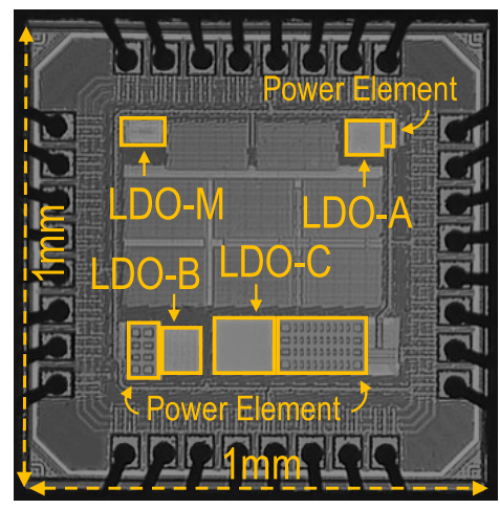 |
The design and verification process for analog circuits can be long and tedious, wherein designers rely heavily on manual effort to create circuits and draw layouts, thereby limiting turn-around-time and design scale and increasing costs. Various previous works have tried to solve this issue by leveraging digital automated place-and-route (APR) tools, but they involve replacing analog elements with digital counterparts, thereby dampening performance. In this work, we propose a digital flow-based approach to design all-analog circuits that dramatically speeds up the design and layout process while retaining the benefits of true analog topologies and demonstrate the performance for three low-dropout regulators (LDOs). Fabricated in 65-nm CMOS, measurement results show that the generated LDOs achieve up to 99.95% peak current efficiency, a figure-of-merit (FOM) of 4.6 ps, and up to 63.93% reduction in input offset variability with respect to their manually designed counterparts. |
 |
A -108dBm sensitivity, 430MHz, 130nW-41µW, 6.25bps-4.2kbps, digitally tunable wake-up and data receiver in 65nm CMOS is presented. Employing 2-tone RF OOK modulation and an AlN MEMS resonator, the receiver attains close-in SIR of -25dB at 0.12% and far-out SIR of -28dB at 0.7% frequency offset from the carrier. Digitally configurable dynamic ranges of 11dB, 410X, 672X are achieved for sensitivity, power, and latency, respectively. The design receives data at a 4.2kbps bit-rate at - 108dBm sensitivity while consuming 41µW. The proposed WuRx is a highly reconfigurable and interference robust candidate for emerging ultra-long range IoT LPWAN applications. |