
 |
A 1 trillion node internet of things (IoT) will require sensing platforms that support numerous applications using power harvesting to avoid the cost and scalability challenge of battery replacement in such large numbers. Our previous SoCs achieve good integration and energy harvesting, but they limit supported applications, need higher end-to-end harvesting efficiency, and require duty-cycling for RF communication. In this project, we demonstrates a highly integrated, flexible SoC platform that supports multiple sensing modalities, extracts information from data flexibly across applications, harvests and delivers power efficiently, and communicates wirelessly. |

The SoC has two main sensing interfaces: a 4-channel (2µW/channel) analog front-end (AFE) with an 8-bit analog-to-digital converter (ADC) and SPI with variable voltage output pads (0.4-to-3.3V) for commercial sensor compatibility. The Opencores MSP430 (OMSP) processor and a suite of accelerators can execute numerous biomedical and environmental signal processing algorithms (e.g. filtering, peak detection, histograms) combining ASIC energy efficiency and flexibility. A Lightweight Control Unit (LCU) can manage chip data and node control while the OMSP is off, and uses a custom instruction set architecture (ISA) and interrupt-driven programs to reduce the program size. The chip’s flexible clocking unit, containing a programmable all digital phase locked loop (ADPLL) and system clock configurability, can drive the system clock from a low power crystal. The digital blocks run in the sub-threshold regime on a 0.5V supply delivered by the PMU. The SoC uses an asymmetric transceiver architecture for data transmission and reception with 1) An ultra wideband (UWB) transmitter and 2) A narrowband wakeup receiver respectively.
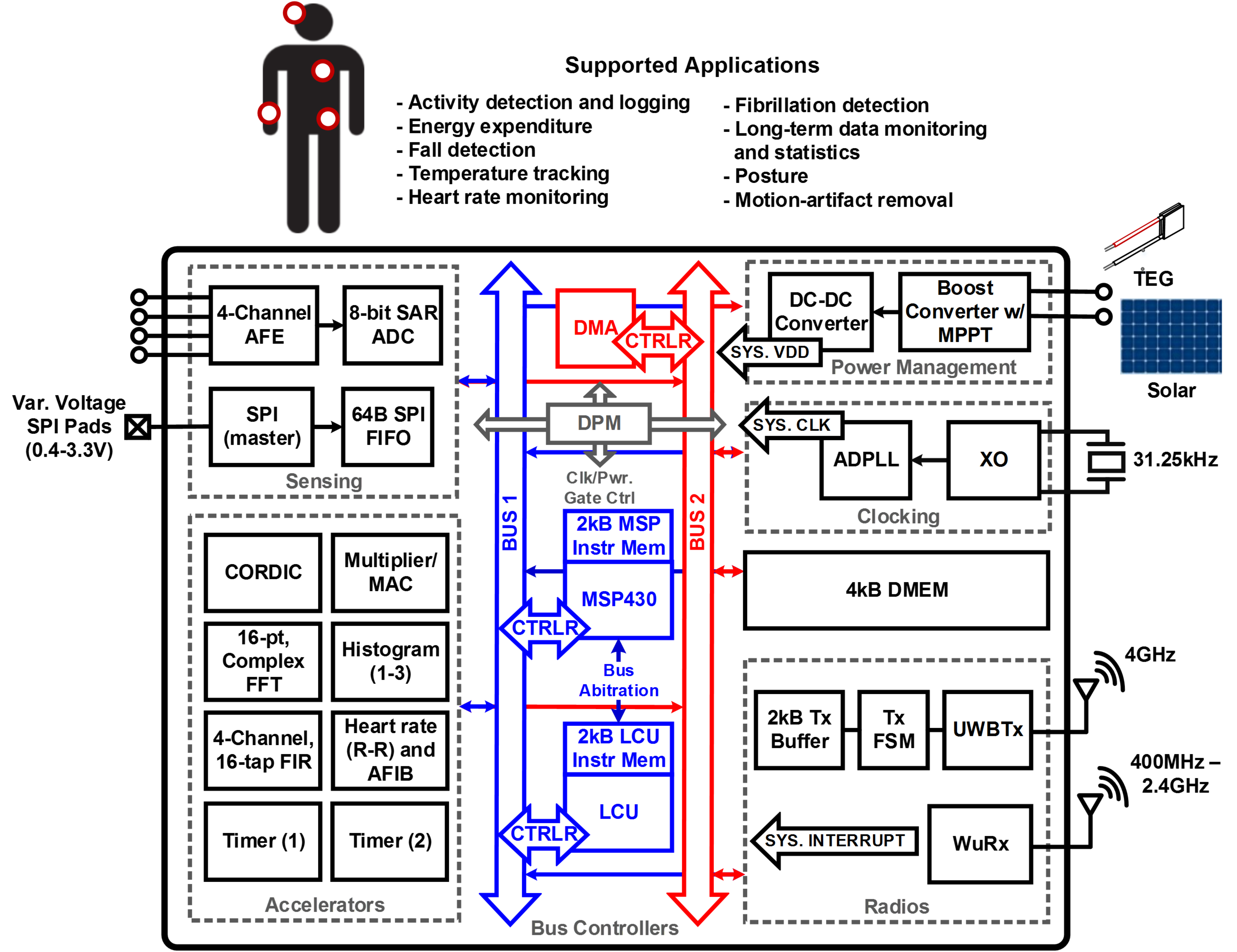

The integrated energy-harvesting and power management unit (EH-PMU) couples a boost converter and a SIMO DC-DC regulator for power delivery to the SoC. The EH-PMU leverages two off-chip high-Q inductors (for the boost converter and the regulator) and an off-chip storage capacitor (or a super-capacitor) for storing harvested energy. The boost converter can harvest from a photovoltaic (PV) solar cell (e.g., with open circuit voltage of 1.7V) or from a TEG (e.g. with input voltage VIN as low as 10mV) and charge the storage capacitor up to VCAP=1.4V. An integrated maximum power point tracking (MPPT) circuit tunes the input impedance of the boost converter to extract maximum energy from the ambient source (either TEG or PV). The SIMO utilizes a buck-boost architecture to provide regulated outputs of 1.2V and 0.5V from a minimum input voltage (VCAP) of 0.7V provides a peak end-end efficiency of 75% at 1.2V output delivering a 100uA load current. Both the SIMO and the boost converter operate in Discontinuous Conduction Mode (DCM) to minimize conduction losses. The control scheme in both the boost converter and the SIMO consists of a peak inductor current control scheme that ensures constant peak current in the inductor with pulse-frequency-modulation (PFM) control to reduce conduction loss and a zero crossing detector to minimize conduction losses across the diode. The PMU also includes a cold-start circuit with a startup voltage of 220mV.
 |
 |

The chip uses two 16-bit independent buses, each controlled by a separate controller. Bus 1 is controlled by either the OMSP or LCU, while Bus 2 is controlled by a two-channel DMA. Both buses have access to all the peripherals within the SoC. At startup, the LCU is the main controller on the chip and can configure the OMSP as the main controller of Bus 1 or as a bus peripheral that is used only for ALU or background operations. The chip has a 4kB data memory and three 2kB memories: the LCU instruction memory, the OMSP instruction memory, and the radio transmitter buffer.
The SoC also has a suite of programmable hardware accelerators to support energy efficient digital operation for common functions including an FIR filter, a CORDIC block, an FFT/IFFT, two timer modules, a multiplier, a histogram, and a heart rate (R-R) / atrial fibrillation (AFIB) detection block.

The SoC also contains a digital power management unit (DPM) that monitors the harvested energy by measuring the voltage on the storage capacitor and controls the different peripherals to ensure that the chip does not lose power when energy-harvesting conditions are poor. The DPM has three voltage thresholds that set the operating mode of the chip (green, yellow, or red). In green mode, the storage capacitor is nearly full, and the chip can perform any functionality. In yellow mode, the storage capacitor is being drained, and the chip must use its energy resources more efficiently. In red mode, the chip is approaching loss of power, and only essential operations must be performed. 
The UWB transmitter (Tx) uses OOK modulation with a data rate of 187.5kbps, chosen to match the data rate of the 802.15.6 WBAN standard. The center frequency is 3.994GHz with a 500MHz bandwidth. It consists of a pulse-width generation circuit to create a short pulse, which is then used to enable/disable a ring oscillator, creating the UWB pulses of period 2ns. A Class AB power amplifier buffers the signal onto the antenna. A finite state machine (Tx FSM) controls the data transfer and contains a 2kB sub-threshold memory buffer that stores the raw data to be transmitted.
To build a low power wakeup receiver (WRX) a narrowband RF link is chosen. A rectifier is used to replace the power hungry LNA and a bank of 31-bit CDMA codes is used for synchronization. From the antenna and band-select filter, the RF signal passes through an off-chip 2-element passive matching network that boosts the signal in 5dB before going into the rectifier. A 30-stage rectifier working in the sub-threshold region is used to directly down convert the RF signal to baseband. To synchronize the transmitted code and issue a wakeup, a bank of four correlators continuously correlates the 4x-oversampled comparator bit-stream with a programmable, 31-bit CDMA code. The baseband processor is synthesized in sub-threshold in order to save power.


To demonstrate maximum power point tracking (MPPT) and system startup, we used a commercial solar cell. It was observed from measurements that the boost converter enabled the MPPT loop to tune the input impedance of the boost converter so that the solar cell is loaded to operate at its maximum power point. After the harvested energy is stored on the storage capacitor, the necessary power can be provided to the SoC for continuous operation. In addition the chip was tested end-to-end for motion capture with an accelerometer while powered from indoor solar by the PMU. Acceleration data is fed to the FIR filter for DC filtering and the output is transmitted over the radio to an aggregator.


Faculty: Ben Calhoun (UVA), David Wentzloff (University of Michigan) Research Scientist: Dilip Vasudevan (UVA) Students: Abhishek Roy (UVA), Farah B. Yahya (UVA), Xing Chen (UMich), Christopher Lukas (UVA), Divya Akella (UVA). UVA Graduated Students: Alicia Klinefelter (Intel), Patricia Gonzalez (UVA), Jim Boley (Psikick), Kyle Criag (Psikick), Yousef Shahsheer (Psikick), Aatmesh Shrivastava (Psikick) UMich Graduated Students: Muhammad Faisal, Seunghyun Oh, Nathan E. Roberts (Psikick)