 |
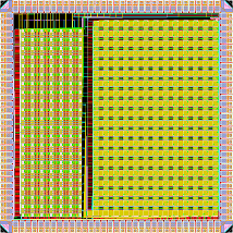
This work explores reconfigurable circuits operating at low voltages. While the existing FPGAs are too high power to meet the requirements of IoT applications, we designed and optimized new circuit typologies of CLBs and global interconnect in near/sun-threshold region. We also developed custom tool flow to support full chip configuration. A 90nm chip implements the FPGA with 1134 LUTs, which is 2.7X smaller, 14X faster, and 4.7X less energy than a sub-threshold FPGA using conventional circuits and 22X less energy than an equivalent FPGA at full VDD. We are currently working towards dynamic voltage scaling and measurements using real-life applications. |
The SubVT FPGA is an effort by the Sub-VT group to explore reconfigurable circuits operating at low voltages. Our initial sub-threshold FPGA chip (90nm bulk CMOS)contains two different FPGAs, each of about 1000 basic logic elements (BLEs) in size. The first FPGA, which we refer to as the "Custom Case," is specifically designed to operate at low-energy. Our research has shown us that the majority of delay and energy is consumed in the global routing network; therefore, our efforts have focused on making the interconnect more efficient. Besides many small optimizations, the main feature of the custom case is the low-swing interconnect links received by a special asynchronous sense amp. In addition, the architecture of the custom-case is designed to be resistant to process, voltage, and temperature variations. The second FPGA, called the "Base-Case" because it is inspired from industry "best-practices" that we optimized for sub-threshold, was built in order to provide a comparison for the Custom Case in the same technology. The Custom-Case is approx 2.5X as area efficient, and simulations (on a benchmark suite of 40 different cases) show it to be much more efficient than the Base Case. The Custom Case in Sub-VT averages 25x less energy compared to the Base Case at 1.2V. When operating at the same energy, the custom-case is approx 7x faster. When operating at the same VDD, the custom-case operates 4.5X faster using 40% less energy.


The FPGA team also explored and optimized the circuit typologies of global interconnect and CLBs. A 130nm test chip implementing low-swing interconnect meshes with different circuit parameters is measured. The results show that optimization of the low-swing interconnect provides up to 60.2% lower energy-delay-product (EDP) than a straightforward, un-optimized design at VDD = 0.4V. Furthermore, the simulation results show that the optimized interconnect is 97.7% faster and 42.7% lower energy than a traditional uni-directional interconnect at VDD = 0.4V. We also compared area, delay, and energy for two intra-CLB topologies: multiplexer-based routing and island-style bi-directional routing, similar to the global FPGA interconnect, but used inside the CLB (which we call a mini-FPGA). The mini-FPGA style of local CLB interconnect prove to be favorable for minimum-energy operation, as they can reduce transistor count by as much as 62%, and consume as much as 77.9% less energy. Multipexer-based CLBs have performance benefits by reducing delays by almost 3x. We are currently working towards dynamic voltage scaling and measurements using real-life applications.
Students: He Qi
