
 |
As energy-constrained systems continue to reduce their power consumption, finding an optimal point of operation for the principle components in the energy budget becomes increasingly important. With energy dominant system components like communication circuits, it is important to consider both energy-per-bit and power in the context of the system’s use cases. In this project, we propose optimization of chip-to-chip links considering both power and energy per-bit to find the optimal operating voltage and activity factor while minimizing wasted energy and power. |
Energy optimization in circuits has become an important field of research due to the demand of ultra-low power (ULP) systems that contribute to the internet of things (IoT). These circuits generally do not have the high throughput requirements of high-power, high-performance chips and must be optimized using different techniques. These emerging technologies have a need for optimally energy efficient I/O for communication with off-chip nodes such as sensing devices, radios, and body area networks. There remains a need to address optimization of low throughput communication. Because of the need to amortize static and leakage energy, current research for chip-to-chip I/O is pushing into higher frequencies to reduce energy-per-bit. The figure below shows that the lowest E/b designs use very high frequencies. As a result, the figure shows the need for lower energy I/O circuits at lower frequencies.

If a power budget is defined for a communication circuit, this optimization results in a maximum activity factor and voltage that can be used to operate within a given system’s budget. Both metrics are important to minimize in the design of an ultra-low power transmission line circuit and can be used together to find an optimal point of operation. In some cases, the minimum energy point produces a throughput that is higher than required for an application. As a result, the circuit's energy can be further reduced through lowering activity factor. This produces a new curve with a new minimum energy point. As fewer cycles are spent transmitting data, the leakage energy dominates the curve and pushes the optimal point to the right, increasing its voltage.

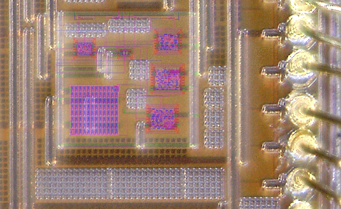
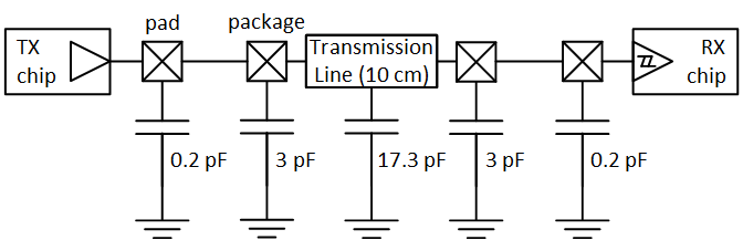
The fabricated chip’s block diagram shown below shows the major sources of capacitance, which decrease the energy efficiency of the circuit. We chose to use a 10 cm trace between the transmitter and receiver to get a pessimistic capacitance on the PCB transmission line. In a non-test environment, the transmission line capacitance can be greatly reduced by both optimizing the distance between the transmitter and receiver, and moving from a PGA package to one with lower internal capacitance.
When used in a system, this communication circuit will ideally be at the bottom left of the below figure, having both a power consumption and energy per bit as close to zero as possible. Pushing to the lower left of the figure is limited by the physical constraints of the circuit, mainly its ability to reduce its operating voltage. Once the minimum operating voltage is found it can be used to find the maximum throughput. The maximum throughput gives the minimum energy-per-bit due to amortization of leakage energy. If this throughput is above the system’s requirement, the best course of action is to travel down the blue line in the figure by reducing activity factor until the throughput matches the budget. If the throughput is below the system’s requirement the voltage can be increased by traveling up the black line, increasing the maximum frequency of the circuit until the necessary throughput is met.
