

Body area sensor networks (BASNs) are rapidly becoming important tools in today's health care. However, the growing trend for portable health care is constrained by flexible on-node processing and very long device lifetimes. Increased life time of these devices will result in reduced cost to consumer and less invasive procedures to replace batteries/nodes. In this project, we utilize the state-of-the-art in low power RF transmitters, low voltage boost circuits, subthreshold processing, biosignal front-ends, dynamic power management, and energy harvesting to realize an integrated reconfigurable wireless body area sensor network (BASN) SoC capable of autonomous power management for BATTERY-FREE operation.

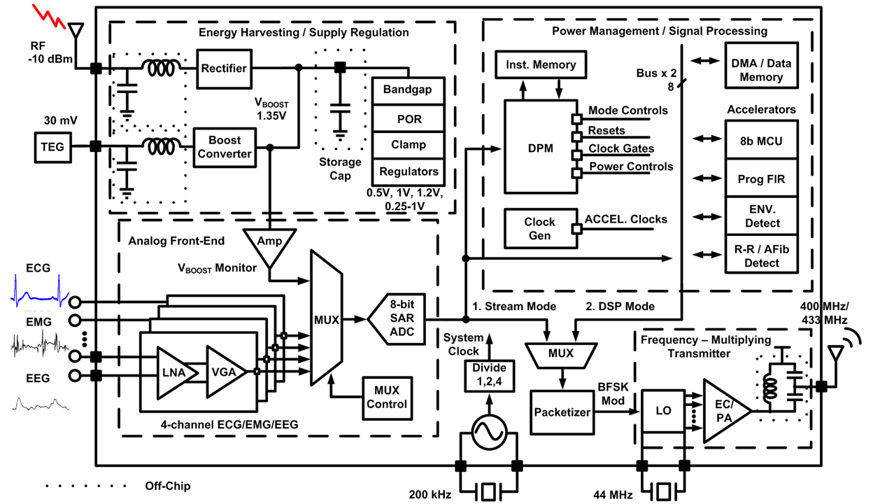
Our chip has many stringent constraints in order to meet our requirements for a battery-less and flexible BASN platform, some of which include: • Ultra low total chip power for sustainable operation using TEG • Voltage regulation to convert ultra low voltage input (10’s mV) to usable voltage, and to supply different voltage domains across the chip • Various analog bio-signal acquisition, amplification, and digitization • Ultra low power, re-programmable digital signal processing for energy efficient adaption of various algorithms • Low power transmission and flexible data rates • Total chip power management for efficient power-steering to the essential circuit components Here is the chip architecture solution to our many challenges:
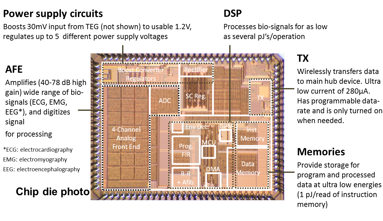
Here are all of the parts explained!
 |
An energy harvesting/supply regulation section boosts an input as low as 30mV up to a regulated 1.35V supply. In the end we use a hybrid energy harvesting subsystem, allowing operation from RF and/or thermoelectric power sources. Small body-worn TEGs typically provide very low output voltages (<100mV), but we employ an ultra-low voltage boost converter capable of boosting voltages as low as 30mV. However, the control circuit to our boost converter will not work until ~600 mV is supplied to it. So solve this problem, a one-time kick-start is provided wirelessly through an RF rectifier front-end with incident power as low as -10dBm. The node will then continue to run indefinitely from the TEG. |
 |
A subthreshold digital section performs data processing, mode control, and power management (including power/clock gating of blocks and dynamic voltage scaling (DVS)) based on the available energy on the storage capacitor that stores the energy harvested from the TEG. The digital section includes a custom digital power management (DPM) processor, general purpose microprocessor (MCU), programmable FIR, 1.5kB instruction SRAM / ROM, 4kB data SRAM, and dedicated accelerators for ECG heart rate (R-R) extraction, atrial fibrillation (AFib) detection, and EMG band energy calculation. This section is truly the 'heart' of the BASN chip. Not only is the DPM available to manage the whole chip, the flexibility of this digital processing subsystem makes it so processing through the MCU, fully custom processing with accelerators, or a mixed approach is readily available based on application needs. The digital subsystem is capable of processing the bio-signals at an ultra low energy consumption in the sub-nanowatt range. |
 |
An analog front-end (AFE) with programmable gain and a successive-approximation (SAR) ADC amplifies and digitizes signals as low as a few μVs. The chip has four independently selectable biosignal input channels. Our amplifiers provide digitally-programmable gain (40-78dB) from DC to 320 Hz at 3μW/channel, compatible across many different bio-signal types. |
 |
We utilize a transmitter architecture that consumes 160µW when transmitting at its maximum data rate of 200 kbps. Though this greatly relieves the transmitter (TX) as being the total chip power hog, it is still not efficient enough to be transmitting at 100% duty cycle and leave enough energy on the storage capacitance for a sustainable battery-less chip. However, the data extraction from the digital signal processing portion, for example running the R-R extraction algorithm reduces the duty cycle and average transmitter power consumption to 0.013% and 190nW respectively. The packetizer contains a programmable packet header and CRC (cyclic redundancy check) to allow compatibility with commercial receivers. |

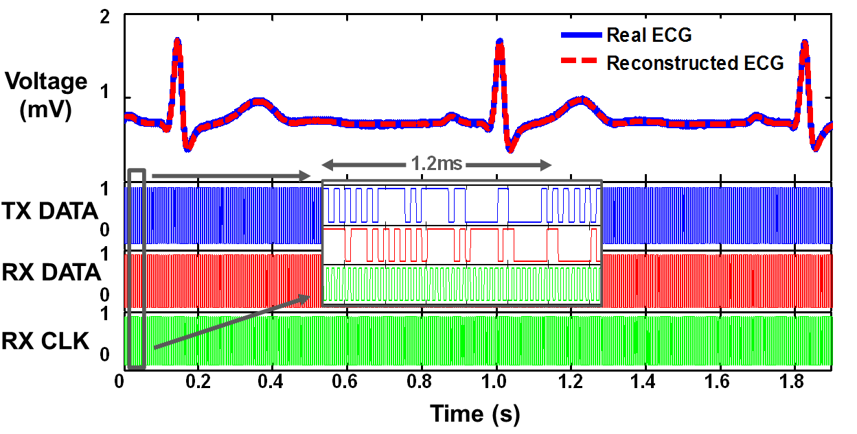
An ECG experiment was performed on a healthy human subject. First, the chip was set to ECG raw data mode (consuming 397μW). Data was transmitted to a TI CC1101 receiver. The reconstructed ECG closely matched the actual ECG (top). Next, the chip used the on-chip R-R interval extractor to transmit measured heartrate every 5s operating from a 30mV supply voltage (bottom). Every 5s, sufficient available energy is checked, in which case the crystal oscillator is enabled for 20ms before the TX transmission (650μs including turn-on time and transmitting 24b). The heart rate extractor algorithm measures the R-R interval with a time resolution of (1/128)s. The total chip power is 19μW. Faculty: Ben Calhoun (UVA), Brian Otis (University of Washington) Students: Yanqing Zhang (UVA), Yousef Shahsheer (UVA), Jim Boley (UVA), Alicia Klinefelter (UVA), Aatmesh Shrivastava (UVA) Helen Zhang (UW), Jason Silver(UW), Manohar Nagaraju (UW), Jagdish Pandey (UW)